Gigabyte twists its RAM slots to fit 24TB of DDR5 sticks into a standard server — AMD EPYC sports an impossible 48 DIMMs in new configs
July 17, 2024
AMD Threadripper 9000 “Shimada Peak” CPU surfaces in shipping manifest — next-gen Zen 5 HEDT chip sports 96 cores and 192 threads
August 27, 2024The first third-party product will tape out in 1H 2025.
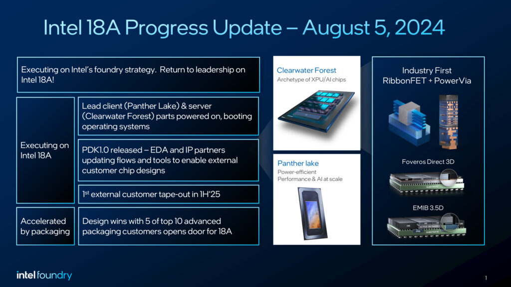
On Tuesday, Intel provided an update on the progress of its 18A (1.8nm-class) fabrication process, a crucial technology for its foundry initiative. By now, the company has a process design kit (PDK) version 1.0 ready, so its third-party customers can start (or even finalize) the development of chips in this manufacturing process. Furthermore, two essential Intel products using this production node have powered on, which is a good sign.
"The Panther Lake client processor is powered on and booting Windows, yielding well, in use inside Intel and ahead of schedule on product qualification milestones," said Kevin O'Buckley, Intel senior vice president and general manager of Foundry Services. "Clearwater Forest [CPU] for datacenter is powered on, booting operating systems, in use inside Intel and performing well."
Intel's 18A is the company's second fabrication technology to use gate-all-around RibbonFET transistors and backside power delivery called PowerVia (particularly crucial for data center-class products that need a lot of power) after 20A. Compared to the 2nm-class manufacturing process, 18A promises optimized RibbonFET design and some other enhancements, which leads to a 10% improvement in performance per watt.
Perhaps more important is that Intel 18A is a process that Intel Foundry's potential customers are very interested in, as it is believed to be more competitive than TSMC's 3nm and 2nm-class offerings available in 2024 – 2025. As a result, it is crucially vital for Intel and its ecosystem partners, such as Ansys, Cadence, Synopsys, and Siemens EDA, to adjust their tools for PDK 1.0 so as to enable Intel's lead customers to finalize their 18A designs that are currently in development and other clients to begin developing their 18A products.


